C H A P T E R  8

Color Graphics Frame Buffer Test (cg14test)

cg14test checks the cg14 frame buffer card. cg14test is specific to the VSIMM (Video SIMM) devices in the SPARCstation 10 SX and the SPARCstation
20 SX.


caution icon

Caution - Do not close the SunVTS window to an icon while it is running frame buffer tests.


cg14test Requirements

Ensure that the frame buffer locking option is enabled from the Options window.

For full instructions on testing frame buffers, see Testing Frame Buffers .


cg14test Groups

There are nine test groups in cg14test :

  1. MDI and VBC Chip Control Registers

  2. Memory Chips

  3. MDI Chip Cursor Registers

  4. MDI Chip CLUT Registers

  5. DAC Chip Registers

  6. MDI Chip XLU Registers

  7. CG14 Display (visual only)

  8. MDI Chip Testmode Readback in 8-bit mode

  9. Driver IOCTLs

TABLE 8-1 cg14 Test Groups

Test Groups

Description

Hardware

(Groups 1-6)

These test groups are tested by opening /dev/fbs/cgfourteenX , mapping the MDI Control Address Space, modifying the target test location (using direct writes to the mapped address space), reading from the mmapped address space for verification, and closing the device.

Visual Pattern

(Group 7)

This subtest loads a visual pattern of 256 colors, then rotates the pattern around. You verify this test by seeing it display.

Data Propagation

(Group 8)

This test group is tested by loading the frame buffer (FB) memory with four neutral data patterns, then setting a target FB pixel with data that triggers the test mode readback latch. The result is read from the readback register after vertical blanking occurs. Two different trigger patterns are used at each FB pixel. All four MDI pixel paths (A - D) are used, and the pixel locations for each trigger are designed to detect gross MDI input data opens or short, VRAM SAM addressing, and VRAM-to-SAM transfer addressing.

The screen shows four horizontal bars, which are either greyscale or colored. These bars change each time the trigger data is inverted, and as it completes the testing of a raster pattern.

Note: If the resolution and VRAM size permits, 8-bits per pixel mode are tested.

Driver (Group 9)

Test all IOCTL calls that have not yet been used to verify proper driver communication to the hardware. Call the driver to perform a hardware update, and then confirm that the update was successful by using the complementary driver read, or reading the mmap'ed address space and comparing it against the stimulus.

cg14test performs the appropriate steps before and after each test (if possible) to maintain context and prevent visual confusion by saving the register data before it is overwritten, disabling video (if possible), performing the specific test, and restoring the saved register data information.

The data used for register testing is optimized to include all 0's, all 1's, and walking a 1 through each bit being tested.

MDI and VBC Chip Control Registers

(Group 1)

  • Master Control Register bits 7-0 write/read verify

  • Packed Pixel Register bits 3-0 write/read verify

  • Master Status Register bits 7-4 read-only verify 0x00 and 0x30 occur

  • Horizontal Blank Start Register bits 9-0 write/read verify

  • Horizontal Blank Clear Register bits 9-0 write/read verify

  • Horizontal Sync Set Register bits 9-0 write/read verify

  • Horizontal Sync Clear Register bits 9-0 write/read verify

  • Composite Sync Clear Register bits 9-0 write/read verify

  • Vertical Blank Start Register bits 11-0 write/read verify

  • Vertical Blank Clear Register bits 11-0 write/read verify

  • Vertical Sync Set Register bits 11-0 write/read verify

  • Vertical Sync Clear Register bits 11-0 write/read verify

  • Transfer Cycle Set Register bits 9-0 write/read verify (MDI revision 0 only)

  • Transfer Cycle Clear Register bits 9-0 write/read verify (MDI revision 0 only)

  • Fault Status Address Register bits 15-0 write/read verify

  • Auto-increment Address Space Register bits 7-0 write/read verify

  • Video Base Register bits 23-12 write/read verify

Memory Chips

(Group 2)

The Memory Chips test group includes VRAM Testing, Memory Retention, and Test Write Recovery.

VRAM Testing:

The Data Bus test uses 18 NTA patterns (Nair, Thatte, and Abraham's testing procedure for RAM) to check for data and address faults. This test is performed in MDI_CHUNKY_XBGR_MAP access mode only. See TABLE 8-2 .

Memory Chips

(Group 2) Continued

VRAM Testing (Continued)

The test ascends through the frame buffer memory, clearing it to 0's. The NTA pattern test number x reads a location to make sure test data y is present. It then writes new data z to that location. The location ascends through the FB sequentially. See TABLE 8-2 .

Memory Retention:

The VRAM Data Retention test checks for gross problems with the VRAM refresh. Since refresh is active during this test, no retention problems should occur unless the refresh is defective.

This test turns off the video, writes 0's to all the VRAM, waits the specified memory_hold time (the default is five seconds), then reads and compares all VRAM data. This process is repeated with data of f's, then the video is restored and the test is complete.

Two command-line parameters are related to this test: R= number and H= number . R= lets the user specify the refresh interval from 128-1023. The time between refresh cycles and the system default is 123. H= lets the user specify the retention test hold time in seconds.

Write Recovery:

A Write Recovery test is used in all the EMC mapping modes to write data to 0's followed by immediately reading that data location to see if the VRAM can recover from a write correctly. This is done to all sequential ascending locations. Next, a second independent pass of memory is made with the complementary data of 0xffffffff written to descending locations of the FB memory buffer.

The EMC mapping access modes are:

  • MDI_CHUNKY_XGBR_MAP

  • MDI_CHUNKY_BGR_MAP

  • MDI_PLANAR_X16_MAP

  • MDI_PLANAR_C16_MAP

  • MDI_PLANAR_X32_MAP

  • MDI_PLANAR_B32_MAP

  • MDI_PLANAR_G32_MAP

  • MDI_PLANAR_R32_MAP

MDI Chip Cursor

Registers (Group 3)

The MDI Chip Cursor Registers are:

  • Cursor Plane 0 Register bits 31-0 write/read verify

  • Cursor Plane 1 Register bits 31-0 write/read verify

  • Cursor Plane 0 Register bits 31-0 write/read verify (with auto increment)

  • Cursor Plane 1 Register bits 31-0 write/read verify (with auto increment)

  • Cursor Control Register bits 2-0 write/read verify

  • Cursor Color Register 1 bits 28-0 write/read verify

  • Cursor Color Register 2 bits 28-0 write/read verify

  • X-Cursor Location Register bits 11-0 write/read verify

  • Y-Cursor Location Register bits 11-0 write/read verify

  • Cursor Plane 0 Non-Auto Registers test

  • Cursor Plane 0 Auto Registers test

  • Cursor Plane 1 Non-Auto Registers test

  • Cursor Plane 1 Auto Registers test

  • Cursor Planes Retry A test

  • Cursor Planes Retry B test

MDI Chip CLUT

Registers (Group 4)

The MDI Chip CLUT Registers are:

  • LUT1 Registers 0-255 bits 31-27 & 23-0 write/read verify

  • LUT1 Registers 0-255 bits 31-27 & 23-0 write/read verify (with auto increment)

  • LUT1D Registers 0-255 bits 31-27 & 23-0 write/read verify

  • LUT1D Registers 0-255 bits 31-27 & 23-0 write/read verify (with auto increment)

  • LUT2 Registers 0-255 bits 31-27 & 23-0 write/read verify

  • LUT2 Registers 0-255 bits 31-27 & 23-0 write/read verify (with auto increment)

  • LUT2D Registers 0-255 bits 31-27 & 23-0 write/read verify

  • LUT2D Registers 0-255 bits 31-27 & 23-0 write/read verify (with auto increment)

  • LUT3 Registers 0-255 bits 31-27 & 23-0 write/read verify

  • LUT3 Registers 0-255 bits 31-27 & 23-0 write/read verify (with auto increment)

  • LUT3D Registers 0-255 bits 31-27 & 23-0 write/read verify

  • LUT3D Registers 0-255 bits 31-27 & 23-0 write/read verify (with auto increment)

DAC Chip Registers (Group 5)

The DAC Chip Registers test group includes the RAMDAC registers and control registers.

RAMDAC Registers:

  • Address Register bits 7-0 (0x7 maximum) write/read verify

  • Mode Register bits 7-0 (skip bit 5) bits write/read verify

Control Registers:

  • ID Register bits 7-0 r/o verify data is 0x8C

  • Pixel-Mask Register bits 7-0 write/read verify (skipped if dac rev= 2)

  • Command2 Register bits 7-0 write/read verify (skipped if dac rev = 2)

  • Command3 Register bits 7-0 write/read verify (skipped if dac rev = 2)

MDI Chip XLUT

Registers (Group 6)

The MDI Chip XLUT Registers are:

  • XLUT Registers 0-255 bits 7-0 write/read verify

  • XLUT Registers 0-255 bits 7-0 write/read verify (with auto increment)

  • XLUTD Registers 0-255 bits 7-0 write/read verify

  • XLUTD Registers 0-255 bits 7-0 write/read verify (with auto increment)

CG14 Display (visual only)

Group 7)

This test visually displays 256 boxes on the screen (each in a different color), and then shifts the CLUT1 entries giving the visual impression of the pattern mirroring itself from left to right horizontally. The pattern then rotates up, down, followed by mirroring itself horizontally left to right.

MDI Chip Test Mode Readback Register (Group 8)

This test mode reads back register bits 23-0 in read-only and verify modes.

Driver IOCTLs (Group 9)

  • MDI_GET_CFGINFO check # of CLUT's, pixel height, pixel width, and pixel mode against hardware

  • FBIOGATTR check real_type , fb_height , fb_width , fb_depth , fb_cmsize , and fb_size against cfginfo values

  • FBIOGTYPE check fb_type , fb_height , fb_width , fb_depth , fb_size , and fb_cmsize against driver defines or cfginfo values

  • FBIOGVIDEO check status returned against hardware

  • FBIOSVIDEO set off, off, on, on, off verifying against hardware

  • FBIOVERTICAL (imbedded in FBIOSVIDEO )

  • MDI_VRT_CNTL turn off, off, on, on, off the video interrupt enable and verify the hardware agrees MDI_SET_PIXELMODE set different modes and verify against the hardware

  • MDI_SET_PPR set the different modes and verify against the hardware

  • MDI_SET_COUNTERS set HSS, HSC, XCC, HBC, XCS, HBS, CSC, VSS, VSC, VBC, VBS, HCT, and VCT then verify against hardware

  • MDI_SET_XLUT set xlut and verify against hardware

  • MDI_GET_XLUT get xlut and verify against hardware

  • MDI_SET_CLUT set clut (1-3 as applicable) and verify against hardware

  • MDI_GET_CLUT get clut (1-3 as applicable) and verify against hardware

  • FBIOPUTCMAP set and verify clut1 matches

  • FBIOGETCMAP verify clut1 matches get

  • FBIOSATTR set emu_type to FBTYPE_MDICOLOR and verify

  • FBIOGATTR check

  • FBIOGCURMAX verify x and y size match driver defines

  • FBIOSCURSOR verify set at 3 locations matches hardware

  • FBIOGCURSOR verify driver knows what set(s) just did

  • FBIOSCURPOS verify set at three locations matches hardware

  • FBIOGCURPOS verify driver knows what set(s) just did

  • MDI_SET_CURSOR set then check CCR, XCU, and YCU cursor hardware registers


TABLE 8-2 cg14test NTA Testing Patterns

NTA Test Pattern

Number = x

Test Data = y

New Data = z

1.0

0x00000000

0x01010101

1.5

0x01010101

0xffffffff

2.1

0xffffffff

0xf1f1f1f1

2.2

0xf1f1f1f1

0x33333333

3.1

0x33333333

0xf0f0f0f0

3.2

0xf0f0f0f0

0x0f0f0f0f

4.1

0x0f0f0f0f

0x55555555

4.2

0x55555555

0xaaaaaaaa

5.1

0xaaaaaaaa

0x05050505 (1x)

0x88888888 (2x)

5.2

0x88888888

0xf5f5f5f5

6.1

0xf5f5f5f5

0x00000000 (1x)

0x5f5f5f5f (2x)

6.2

0x5f5f5f5f

0x11111111

7.1

0x11111111

0x00000000 (1x)

0xcccccccc (2x)

7.2

0xcccccccc

0xdbdbdbdb

8.1

0xdbdbdbdb

0x6d6d6d6d

8.2

0x6d6d6d6d

0x6b6b6b6b

9.1

0x6b6b6b6b

0x0000000

9.2

0x00000000

-


cg14test Options

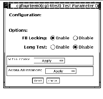
To reach the dialog box below, right-click on the test name in the System Map and select Test Parameter Options. If you do not see this test in the System Map, you might need to expand the collapsed groups, or your system may not include the device appropriate to this test. Refer to the SunVTS User's Guide for more details.

FIGURE 8-1 cg14test Test Parameter Options Dialog Box

TABLE 8-3 cg14test Options

Options

Description

FB Locking

See Testing Frame Buffers for details.

Long Test

When enabled, the color bar screen(s) in the MDI Testmode Readback test checks all SAM transfers in clock=0 mode and clock=1 mode. If Long test is disabled, clock=1 runs checks on the first eight addresses and the first SAM transfer only.

Processor Affinity

For multiprocessor systems, indicates the processor to be tested.


cg14test Test Modes

Due to the nature of graphic tests, reading from or writing to the frame buffer during graphic tests will disturb user operation. This test is only available in offline Functional test mode.

TABLE 8-4 cg14test Test Modes

Test Mode

Supported?

Description

Connection

No

Not supported.

Functional

(Offline)

Yes

This mode uses all subtests to test the cg14 frame buffer. The user can select the long mode for TRMB subtest.


cg14test Command-Line Syntax

/opt/SUNWvts/bin/cg14test standard_arguments -o dev= device_name , lock= E(nable)/D(isable) ,L,I

TABLE 8-5 cg14test Command-Line Syntax

Argument

Description

dev= device_name

Specifies the path of the cg14 device file to be tested;
for example: /dev/fbs/ device_name.

lock= E(nable)/D(isable)

Enables and disables the window system locking option. See Testing Frame Buffers for details. Do not use when your device is the window system display.

L

Enables the long TMRB test.

I

Enables optional driver ioctl tests for cursor.
Note: Do not move the mouse during the cg14test when you run this option.


Note Note - 64-bit tests are located in the sparcv9 subdirectory: /opt/SUNWvts/bin/sparcv9/testname. If a test is not present in this directory, then it may only be available as a 32-bit test. For more information refer to 32-Bit and 64-Bit Tests.